
Research
Microscopy and Nanoscopy
The wavelength range of the light visible to human eyes is about 400~700 nm. The classical optical microscopes work best in this wavelength range, however, the resolving powers of these microscopes are limited by the wave nature of light. Until recently, optical microscopy provided an image with resolution ~500 nm in the visible wavelength of light. In recent years, apertureless type probes, such as a cantilever of atomic force microscope (AFM), a metallic probe of STM, and a small metal particle, have been exploited for the achievement of much higher spatial resolution ~30 nm. The potential for improved spatial resolution is tremendous because an apertureless probe may be approximated as one or a few dipoles that interact locally with a sample surface. Above all, the metal nano-structures strongly enhance the local filed due to excitation of surface free electrons and help to improve the sensitivity of the measurements. We are developing a near-field optical microscopy and related measurement techniques. Our final goal is to construct a microscope to see nano world easily just like watching TV.
顕微分光
顕微鏡を使うと、肉眼では見えない小さい物体を観察することができます。これは、観察対象が可視光の下でどんな姿をしているかについての情報を与えてくれます。同時に試料が空間的にどのように分布しているか、ということを知ることもできます。例えば、ポリマー材料について混合がうまくいっているか、半導体結晶において肝心な機能を発現しているのはどの構造か、生物試料においてどの分子とどの分子が近くにいて相互作用をしているかなどを評価することができます。光学顕微鏡は可視光を用いているので、各種の分光法を同時に行うことで試料を構成している分子を分析することができます。物質の姿を見るだけでなく構成分子まで分かるので、非常にパワフルな分析手法と言うことができます。顕微分光には通常の分光技術とは異なる様々なテクニックがあり、当研究室ではそのような顕微分光技術の開発、すなわち”顕微鏡を作る仕事”を行っています。
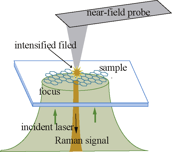
近接場光学顕微鏡
通常の光学顕微鏡の空間分解能は光の波長によってその上限が制限されており、可視光ならだいたい500 nm程度です。光が波の性質をもっているために、これより小さい物体を見ることはできません。当研究室では様々な顕微鏡を開発していますが、特に力を入れているのは近接場光学顕微鏡です。近接場顕微鏡では、小さい針の先端に光をあて、その針で試料をなぞっていくことで光学画像を取得します。ここで空間分解能を決めているのは小さい針先端の大きさです。針先端は、エッチング技術によって~10 nm以下まで小さくすることができます。小さくて尖った針の先端は光をあてるとよく光るので、明るい微小光源として利用することができます。これをピエゾ素子という装置にとりつけて少しずつ動かしていけば、画像を取得することができます。分光測定と組み合わせれば、超解像の組成地図を作成することができます。近接場光学顕微鏡は一般の人が気楽に使える道具ではありませんが、技術を改善して、多くの人に可視光で見たナノスケールの世界を身近に感じてもらえるようにしたいと考えています。
Optical properties of nanomaterials
Recently, there has been a strong demand to examine the optical and electronic properties of nano-materials because of their superb functions due to their size and surface chemical properties. For example, semiconductor nanocrystals e.g. titanium dioxide has been widely used as a photocatalyst for variety of environmental applications such as energy creation, photovoltaic device fabrication, self-cleaning, water disinfection, and air purification. Improving the activity of such semiconductor nanocrystal has become a frequent topic of discussion. The band structure of semiconductor naocrystal is modulated when the size is smaller than several tens of nanometers, owing to crystallinity and quantum size effects. The size-dependent bandgap has been studied as an ensemble average of crystals prepared with a narrow size distribution through X-ray crystallography or UV– vis absorption spectroscopy and spectroscopy. Microscopic observation of individual nanocrystals will provide a better understanding of the relationship between the bandgap and structural parameters such as size, crystallinity, and shape. We are developing a microscopic method to observe individual nanocrystals exhibited intrinsic bandgaps depending on their unique structure for future applications of these materials such as photocatalysis, photoelectric conversions, optical sensors and detectors.
ナノ材料の光物性
試料のサイズが小さくなっていくと、物性も変化していきます。例えば半導体ナノ結晶において、サイズが10 nm付近まで小さくなると、バンドギャップが広がってくるという現象が見られます。また、ナノ材料においては表面積の占める割合が体積にくらべて多くなって、反応性が変わってくることもあります。大きな結晶に比べてナノ結晶は、一つひとつがサイズ形状効果による変調を受けて、個性が際立っていると言う事ができます。近年、光電子変換材料、化粧品や医薬品の開発研究において、このようなナノ材料の物性評価を行う方法が求められています。我々の研究室では、紫外光領域でこのようなナノ材料の光学特性を評価できる特別な顕微鏡を開発して、一個一個のナノ材料を測定しています。実際に測定してみると、人間一人一人と同じくこれらのナノ材料は個性的です。
当研究室では、プラズマ及びレーザーアブレーション法によって、半導体光触媒材料を中心にナノ材料の作製を行っています。液体中に入れた素材にパルスレーザーを照射すると、局所的にアブレーションがおこって素材が微細化すると同時に、酸化還元などの化学反応が誘発されて目的の物質が生成します。
金属ナノ構造の作製も行っています。金や銀などの貴金属はたくさんの自由電子を持っていて、光があたると自由電子が一緒に揺さぶられながら同時に光電場を増幅するという現象が生じます。条件をうまくコントロールしてやると、光は金属表面近傍において桁違いに強くなります。プラズマと呼ばれる電離気体を生成させてこれを金属薄膜にあてると、表面をちょうど良い感じのでこぼこにすることができます。このような金属ナノ構造を使って、先にお話した顕微分光の感度を改善するという研究を行っています。
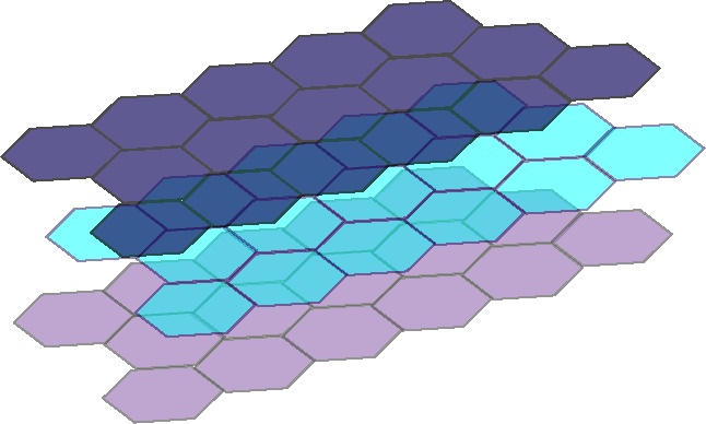
Atomically-thin-layered materials has attracted remarkable interest for their novel physical properties due to unique structures. For example, graphene has been widely studied for its application in semiconductor devices, since the carrier mobility has been reported to be 100 times higher than that of silicon. Graphene consist of atomically thin layers where the each layers has been stacked regularly through van der Waals force. However weak, the interlayer interactions substantially affect the band structure of the materials. It have also been reported that these interlayer space can be intercalated with other molecules, suggesting the possibility for designing a new type of crystal. We are interested in the interlayer interaction of atomically layered materials for designing complex nano-materials as well a new target of vibrational spectroscopy. Our approach is Raman spectroscopy where the system was specifically modified for the observation of low-frequency Raman modes by effectively reject the Rayleigh background.